
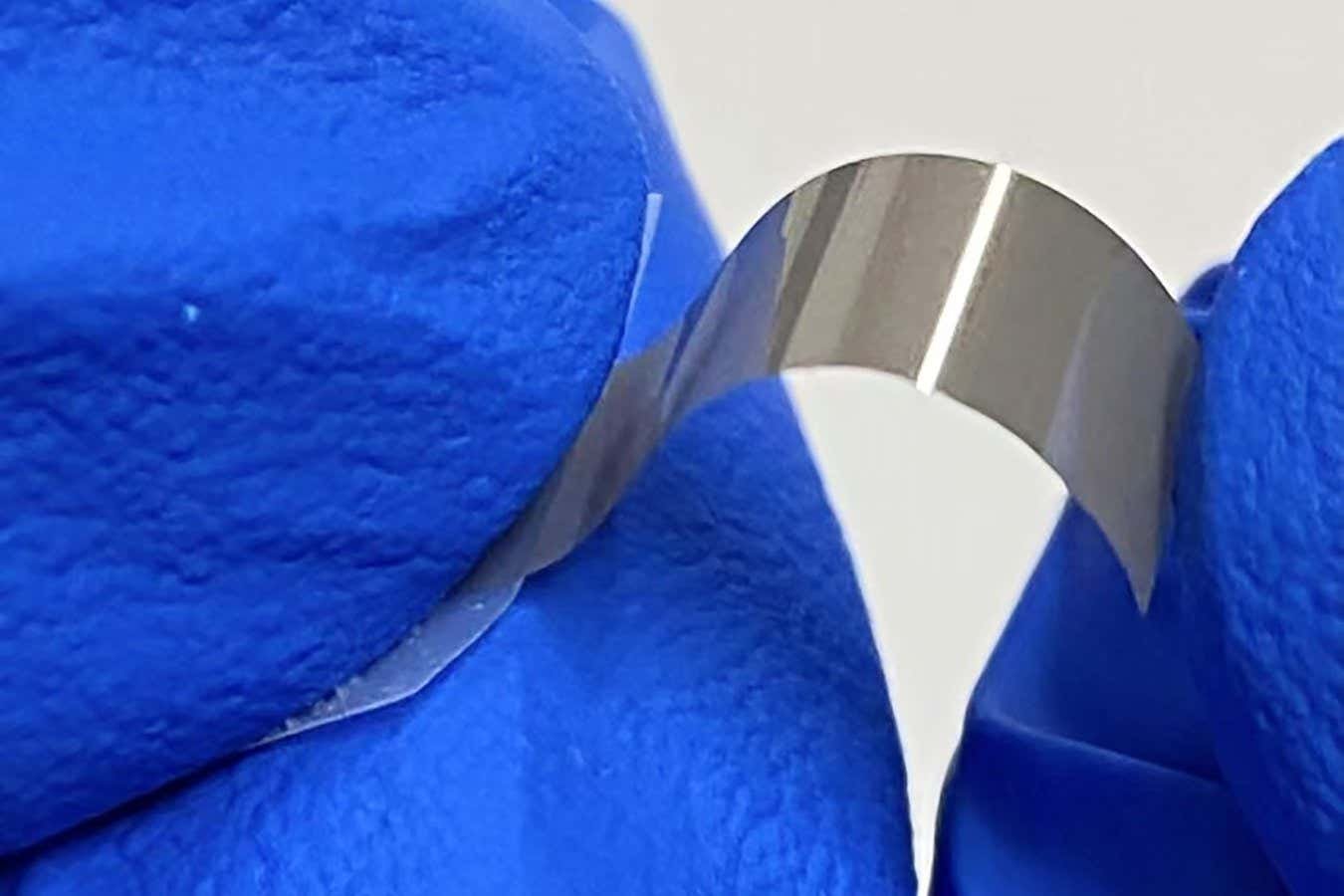

This thin wafer of diamond is also very flexible
Nature, DOI: 10.1038/s41586-024-08218-x
A new way to make ultra-thin diamond wafers using sticky tape could help produce diamond-based electronics, which might one day be a useful alternative to silicon-based designs.
Diamond has unusual electronic properties: it is both a good insulator and allows electrons with certain energies to move with little resistance. This can translate to being able to handle higher energies with greater efficiency than conventional silicon chip designs.
However, producing working diamond chips requires large and very thin wafers, similar to the thin silicon wafers used to build modern computer chips, which have proved tricky to create.
Now, Zhiqin Chu at the University of Hong Kong and his colleagues have found a way to produce extremely thin and flexible diamond wafers, using sticky tape.
Chu and his colleagues first implanted nano-sized diamonds in a small silicon wafer, then blew methane gas over it at high temperatures to form a continuous, thin diamond sheet. They then created a small crack on one side of the attached diamond sheet, before peeling off the diamond layer using regular sticky tape.
They found that this peeled diamond sheet was both extremely thin, at less than a micrometre, much thinner than a human hair, and smooth enough to allow for the kind of etching techniques used to produce silicon chips.
“It is very reminiscent of the early days of graphene when Scotch tape was used to produce the first monolayer of graphene from graphite. I just never would have imagined the concept being applied to diamond,” says Julie Macpherson at the University of Warwick, UK.
“This new edge-exposed exfoliation method will be an enabler for a multitude of device designs and experimental approaches,” says Mete Atatüre at the University of Cambridge. One area it could be particularly useful for is offering greater control in quantum devices that use diamonds as sensors, he says.
The diamond membranes Chu and his colleagues can produce are about 5 centimetres across, which shows that the method works as a proof of principle, says Andrea Ferrari at the University of Cambridge, but it is still smaller than the larger 20-30 centimetres that is standard to many wafer processes, and it isn’t clear whether the new method can be scaled up, he says.
The wafers produced also appear to be polycrystalline, which are less smooth and regular than monocrystalline diamond, and this could limit its use for some applications, says Macpherson.
Topics:

Felecia Phillips Ollie DD (h.c.) is the inspiring leader and founder of The Equality Network LLC (TEN). With a background in coaching, travel, and a career in news, Felecia brings a unique perspective to promoting diversity and inclusion. Holding a Bachelor’s Degree in English/Communications, she is passionate about creating a more inclusive future. From graduating from Mississippi Valley State University to leading initiatives like the Washington State Department of Ecology’s Equal Employment Opportunity Program, Felecia is dedicated to making a positive impact. Join her journey on our blog as she shares insights and leads the charge for equity through The Equality Network.


